Product overview
Key Benefits
Mainlined OpenSTLinux Distribution
One OpenSTLinux Software compatible with STM32MPU Family. OpenSTLinux expansion packages can be applied on the top to enable the use of additional components.
DDR3L support for market advantage
On top of the DDR4/LPDDR4, the STM32MP2 Series supports DDR3L memory, enabling you to maintain competitive pricing and secure supply amid DDR4/LPDDR4 shortages and price surges observed since middle of 2025.
Enhanced security
Advanced security features with SESIP3 target certification supporting security functions for IoT and industrial applications.
Description
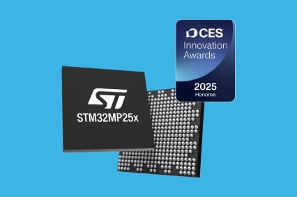
STM32MP25xC/F devices are based on the high-performance single or dual-core Arm® Cortex®-A35 64-bit RISC core operating at up to 1.5 GHz. The Cortex®‑A35 processor includes a 32-Kbyte L1 instruction cache for each CPU, a 32-Kbyte L1 data cache for each CPU, and a 512-Kbyte L2 cache. The Cortex®‑A35 processor uses a highly efficient 8-stage in-order pipeline that has been extensively optimized to provide full Armv8-A features while maximizing area and power efficiency.
STM32MP25xC/F devices also embed a Cortex®-M33 32-bit RISC core operating at up to 400 MHz frequency. The Cortex®-M33 core features a floating point unit (FPU) single precision which supports Arm® single-precision data-processing instructions, and data types. The Cortex®-M33 supports a full set of DSP instructions, TrustZone®, and a memory protection unit (MPU) which enhances application security.
The devices also embed a Cortex®-M0+ 32-bit RISC core operating at up to 200 MHz frequency (16 MHz when running from backup regulator). This processor is located in the SmartRun domain, and can be used to ensure very-low-power peripheral activity when all other processors and domains are stopped.
STM32MP25xC/F devices can also embed a 3D graphic processing unit (VeriSilicon®, OpenGL ES 3.1, Vulkan 1.3, OpenCL 3.0, OpenVX 1.3) running at up to 900 MHz, with performances up to 150 Mtriangle/s, 900 Mpixel/s.
The graphic processing unit can provide a neural processor unit (VeriSilicon®, TensorFlowLite, ONNX, Linux NN) running at up to 900 MHz.
STM32MP25xC/F devices provide an external SDRAM interface supporting external memories up to 32‑Gbit density (4 Gbytes), 16- or 32-bit DDR3L up to 1066 MHz, 16- or 32-bit LPDDR4 or DDR4 up to 1200 MHz. The SDRAM content can be encrypted with AES-128.
The devices incorporate high-speed embedded memories: 808 Kbytes of internal SRAM (including 256-Kbyte AXI SYSRAM, 128-Kbyte AXI video SRAM (which can be used as general purpose), two banks of 128 Kbytes each of AHB SRAM, three banks of 8, 8, and 16 Kbytes of AHB SRAM in SmartRun domain, 128 Kbytes of AHB SRAM in backup domain, and 8 Kbytes of SRAM in backup domain), as well as an extensive range of enhanced I/Os and peripherals connected to APB buses, AHB buses, a 32-bit multi-AHB bus matrix, and a 128/64-bit multi-layer AXI interconnect supporting access to internal and external memories.
Each device offers three ADCs, a low-power secure RTC, 12 general-purpose 16-bit timers, 4 general-purpose 32‑bit timers, three PWM timers for motor control, five low-power timers, and a true random number generator (RNG) , and cryptographic acceleration cells.
STM32MP25xC/F devices offer a video encoder and a video decoder.
The devices support 8 multi-function digital filters (MDF), and one dedicated audio-digital filter with sound-activity detection (ADF).
The devices feature the following standard and advanced communication interfaces.
Standard peripherals
- eight I2Cs
- four I3Cs
- four USARTs and five UARTs
- one low-power UART
- eight SPIs, three I2Ss full-duplex controller/target. The I2S peripherals can be clocked via a dedicated internal audio PLL or via an external clock.
- four SAI serial audio interfaces
- one SPDIF Rx interface
- three SDMMC interfaces
- an USB 2.0 Host with embedded Hi-Speed PHY
- an USB 2.0/3.0 dual-role data with both Hi-Speed and 5Gbits/s SuperSpeed PHYs
- three FDCAN interfaces, including one supporting TTCAN mode (optional)
- two Gigabit Ethernet Interface, with TSN support (optional)
- one Gigabit Ethernet Switch connected to ETH1 and providing two external PHY interfaces, with TSN support (optional)
Advanced peripherals including
- a flexible memory control (FMC) interface
- two Octo-SPI flash memory interface , with on-the-fly content decryption
- two camera interfaces for CMOS sensors, one with basic ISP, demosaicing and parallel or MIPI CSI interface
- an LCD-TFT display interface
- a MIPI DSI display interface (optional)
- an LVDS display interface (optional)
A comprehensive set of power-saving mode allows the design of low-power applications.
STM32MP25xC/F devices are proposed in various packages up to 436 balls with 0.5 mm to 0.8 mm pitch. The set of included peripherals can change with the selected device.
These features make STM32MP25xC/F devices suitable for a wide range of consumer, industrial, white goods and medical applications.
-
All features
- Includes ST state-of-the-art patented technology.
- Cores
- Up to 64-bit dual-core Arm® Cortex®-A35
- Up to 1.5 GHz
- 32-Kbyte I + 32-Kbyte D level 1 cache for each core
- 512-Kbyte unified level 2 cache
- Arm® NEON™ and Arm® TrustZone®
- 32-bit Arm® Cortex®-M33 with FPU/MPU
- Up to 400 MHz
- L1 16-Kbyte I / 16-Kbyte D
- Arm® TrustZone®
- 32-bit Arm® Cortex®-M0+ in SmartRun domain
- Up to 200 MHz (up to 16 MHz in autonomous mode)
- Up to 64-bit dual-core Arm® Cortex®-A35
- Memories
- External DDR memory up to 4 Gbytes
- Up to DDR3L-2133 16/32-bit
- Up to DDR4-2400 16/32-bit
- Up to LPDDR4-2400 16/32-bit
- 808-Kbyte internal SRAM: 256-Kbyte AXI SYSRAM, 128-Kbyte AXI video RAM or SYSRAM extension, 256-Kbyte AHB SRAM, 128-Kbyte AHB SRAM with ECC in backup domain, 8-Kbyte SRAM with ECC in backup domain, 32 Kbytes in SmartRun domain
- Two Octo-SPI memory interfaces
- Flexible external memory controller with up to 16-bit data bus: parallel interface to connect external ICs, and SLC NAND memories with up to 8-bit ECC
- External DDR memory up to 4 Gbytes
- Security/safety
- Secure boot, TrustZone® peripherals, active tamper, environmental monitors, display secure layers, hardware accelerators
- Complete resource isolation framework
- Reset and power management
- 1.71 to 1.95 V and 2.7/3.0 to 3.6 V multiple section I/O supply
- POR, PDR, PVD, and BOR
- On-chip LDO and power-switches for RETRAM, BKPSRAM, VSW, and SmartRun domains
- Dedicated supplies for Cortex®-A35 and GPU/NPU (if present)
- Internal temperature sensors
- Low-power modes: Sleep, Stop, and Standby
- DDR memory retention in Standby mode
- Controls for PMIC companion chip
- Low-power consumption
- Clock management
- Internal oscillators: 64 MHz HSI, 4/16 MHz MSI, 32 kHz LSI
- External oscillators: 16-48 MHz HSE, 32.768 kHz LSE
- Up to 8× PLLs with fractional mode
- General-purpose inputs/outputs
- Up to 172 secure I/O ports with interrupt capability
- Up to 6 wake-up inputs
- Up to 8 tamper input pins + 8 active tampers output pins
- Up to 172 secure I/O ports with interrupt capability
- Interconnect matrix
- Bus matrices
- 128-, 64-, 32-bit STNoC interconnect, up to 600 MHz
- 32-bit Arm® AMBA® AHB interconnect, up to 400 MHz
- Bus matrices
- 4 DMA controllers to unload the CPU
- 48 + 4 physical channels in total
- 3× dual master port, high-performance, general-purpose, direct memory access controller (HPDMA), 16 channels each
- 1× low-power DMA controller with 4 channels in SmartRun domain
- Up to 51 communication peripherals
- 8× I2C FM+ (1 Mbit/s, SMBus/PMBus®)
- 4× I3C (12.5 Mbit/s)
- 5× UART + 4× USART (12.5 Mbit/s, ISO7816 interface, LIN, IrDA, SPI) + 1× LPUART
- 8× SPI (50 Mbit/s, including 3 with full duplex I2S audio class accuracy via internal audio PLL or external clock)(+2 with OCTOSPI + 4 with USART)
- 4× SAI (stereo audio: I2S, PDM, SPDIF Tx)
- SPDIF Rx with 4 inputs
- 3× SDMMC up to 8-bit (SD/e•MMC™/SDIO)
- Up to 3× CAN controllers supporting CAN FD protocol, out of which one supports time-triggered CAN (TTCAN)
- 1× USB 2.0 high-speed Host with embedded 480 Mbits/s PHY
- 1× USB 2.0/3.0 high-speed/SuperSpeed dual role data with embedded 480 Mbits/s and 5 Gbits/s PHY (5 Gbits/s PHY shared with PCI Express)
- 1× USB Type-C® Power Delivery control with two CC lines PHY
- 1 × PCI Express with embedded 5 Gbits/s PHY (PHY shared with USB 3.0 SuperSpeed)
- Up to 3× Gigabit Ethernet interfaces
- 1× Gigabit Ethernet GMAC with one PHY interface (optional)
- 1× Gigabit Ethernet GMAC with one external PHY interface, optionally internally connected to one embedded Ethernet switch providing two external PHY interfaces
- TSN, IEEE 1588v2 hardware, MII/RMII/RGMII
- Camera interface #1 (5 Mpixels at 30 fps)
- MIPI CSI-2®, 2× data lanes up to 2.5 Gbit/s each
- 8- to 16-bit parallel, up to 120 MHz
- RGB, YUV, JPG, RawBayer with Lite-ISP
- Lite-ISP, demosaicing, downscaling, cropping, 3 pixel pipelines
- Camera interface #2 (1 Mpixels at 15 fps)
- 8- to 14-bit parallel, up to 80 MHz
- RGB, YUV, JPG
- Cropping
- Digital parallel interface up to 16-bit input or output
- 7 analog peripherals
- 3 × ADCs with 12-bit max. resolution (up to 5 Msps each, up to 23 channels)
- Internal temperature sensor (DTS)
- 1× multifunction digital filter (MDF) with up to 8 channels/8 filters
- 1× audio digital filter (ADF) with 1 filter and sound activity detection
- Internal (VREFBUF) or external ADC reference VREF+
- Graphics
- Optional 3D GPU: VeriSilicon® - Up to 900 MHz
- OpenGL® ES 3.1 - Vulkan 1.3
- OpenCL™ 3.0, OpenVX™ 1.3
- Up to 150 Mtriangle/s, 900 Mpixel/s
- LCD-TFT controller, up to 24-bit // RGB888
- Up to FHD (1920 × 1080) at 60 fps
- 3 layers including a secure layer
- YUV support, 90° output rotation
- Optional MIPI DSI®, 4× data lanes, up to 2.5 Gbit/s each
- Up to QXGA (2048 × 1536) at 60 fps
- Optional FPD-1 and OpenLDI JEIDA/VESA (LVDS), up to 2× links of 4× data lanes, up to 1.1 Gbit/s per lane
- Up to QXGA (2048 × 1536) at 60 fps
- Optional 3D GPU: VeriSilicon® - Up to 900 MHz
- Artificial intelligence
- Optional NPU: VeriSilicon® - Up to 900 MHz
- TensorFlowLite - ONNX - Linux NN
- Optional NPU: VeriSilicon® - Up to 900 MHz
- Video processing
- Optional hardware video encoder and decoder up to 600 MHz
- H264/VP8 up to FHD (1920×1080) at 60 fps
- JPEG up to 500 Mpixel/s
- 128 Kbytes of video RAM
- Optional hardware video encoder and decoder up to 600 MHz
- Up to 34 timers and 7 watchdogs
- 4× 32-bit timers with up to 4 IC/OC/PWM or pulse counter and quadrature (incremental) encoder input
- 3× 16-bit advanced motor control timers
- 10× 16-bit general-purpose timers (including 2 basic timers without PWM)
- 5× 16-bit low-power timers
- Secure RTC with subsecond accuracy and hardware calendar
- Up to 2× 4 Cortex®-A35 system timers (secure, non-secure, virtual, hypervisor)
- 2× SysTick Cortex®-M33 timer (secure, non-secure)
- 1× SysTick Cortex®-M0+ timer
- 7× watchdogs (5× independent and 2× window)
- Hardware acceleration
- AES-128, -192, -256, DES/TDES
- Secure AES-256 with SCA
- RSA, ECC, ECDSA with SCA
- HASH (SHA-1, SHA-224, SHA-256, SHA3), HMAC
- True random number generator
- CRC calculation unit
- “On-the-fly” DDR encryption/decryption (AES-128)
- “On-the-fly” OTFDEC Octo-SPI flash memory decryption (AES-128)
- Debug mode
- Arm® CoreSight™ trace and debug: SWD and JTAG interfaces
- 12288-bit fuses including 96-bit unique ID
- All packages are ECOPACK2 compliant
Circuit Diagram

You might also like...
EDA Symbols, Footprints and 3D Models
All resources
| Resource title | Version | Latest update | Actions | Details | Download |
|---|
HW Models (1)
| Resource title | Version | Latest update | Actions | Options | ||
|---|---|---|---|---|---|---|
| ZIP | 8.0 | 31 Mar 2026 | 31 Mar 2026 |
System View Description (1)
| Resource title | Version | Latest update | Actions | Options | ||
|---|---|---|---|---|---|---|
| ZIP | 1.2 | 05 May 2025 | 05 May 2025 |
IBIS models (1)
| Resource title | Version | Latest update | Actions | Options | ||
|---|---|---|---|---|---|---|
| ZIP | 3.4 | 23 Apr 2026 | 23 Apr 2026 |
BSDL files (1)
| Resource title | Version | Latest update | Actions | Options | ||
|---|---|---|---|---|---|---|
| ZIP | 3.0 | 15 Oct 2025 | 15 Oct 2025 |
Quality and Reliability
| Part Number | Marketing Status | Package | Grade | RoHS Compliance Grade | Longevity Commitment | Longevity Starting Date | Material Declaration** |
|---|---|---|---|---|---|---|---|
| STM32MP251CAI3 | Active Product is in volume production. | TFBGA 436 18x18x1.2 P 0.8 mm | Industrial | Ecopack2 | 10 | 2026-01-01T00:00:00.000+01:00 | |
| STM32MP251CAJ3 | Active Product is in volume production. | TFBGA 361 16x16x1.2 P 0.8 mm | Industrial | Ecopack2 | 10 | 2026-01-01T00:00:00.000+01:00 | |
| STM32MP251CAK3 | Active Product is in volume production. | VFBGA 424 14x14x1.0 P 0.5 mm | Industrial | Ecopack2 | 10 | 2026-01-01T00:00:00.000+01:00 | |
| STM32MP251CAL3 | Active Product is in volume production. | VFBGA 361 10x10X1.0 P 0.5 mm | Industrial | Ecopack2 | 10 | 2026-01-01T00:00:00.000+01:00 | |
STM32MP251CAI3
Package:
TFBGA 436 18x18x1.2 P 0.8 mmMaterial Declaration**:
STM32MP251CAL3
Package:
VFBGA 361 10x10X1.0 P 0.5 mmMaterial Declaration**:
(**) The Material Declaration forms available on st.com may be generic documents based on the most commonly used package within a package family. For this reason, they may not be 100% accurate for a specific device. Please contact our sales support for information on specific devices.

You’re now leaving st.com and will be re-directed to our Partner’s website.
For the latest innovations and solutions from ST, sign up for our newsletters.
Sample & Buy

| Part Number | Marketing Status | Budgetary Price (US$)*/Qty | Order from ST | Order from distributors | Package | Packing Type | RoHS | Country of Origin | ECCN (US) | ECCN (EU) | Operating Temperature (°C) (min) | Operating Temperature (°C) (max) | Junction Temperature (°C) (min) | Junction Temperature (°C) (max) | |
|---|---|---|---|---|---|---|---|---|---|---|---|---|---|---|---|
| STM32MP251CAJ3 | | | distributors No availability of distributors reported, please contact our sales office |
|
| ||||||||||
| STM32MP251CAL3 | | | distributors No availability of distributors reported, please contact our sales office |
|
| ||||||||||
| STM32MP251CAK3 | | | distributors No availability of distributors reported, please contact our sales office |
|
| ||||||||||
| STM32MP251CAI3 | | | distributors No availability of distributors reported, please contact our sales office |
|
|

STM32MP251CAJ3 Active
STM32MP251CAL3 Active
STM32MP251CAK3 Active
STM32MP251CAI3 Active
(*) Suggested Resale Price (USD) per defined quantity for BUDGETARY USE ONLY. For quotes, prices in local currency, please contact your local ST Sales Office or our Distributors


