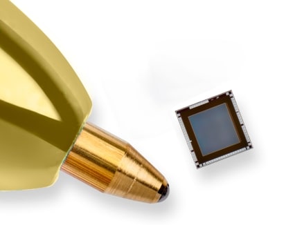
Product overview
Key Benefits

Capture crystal-clear images
Advanced 2.61µm global shutter fully encapsulated pixels providing exceptional sensitivity and sharpness from visible to near-infrared (850nm, 940nm).

Embedded vision ready
Compact and power-efficient design with advanced 3D-stacking and MIPI CSI-2 interface, ideal for ergonomic, battery-powered camera devices on embedded processors.

Quick and easy development
Jumpstart your project with comprehensive evaluation hardware (promodules, S-Board, and more) and free software tools, including evaluation software, SDK, and drivers.
-
All features
- Global shutter technology, STMicroelectronics proprietary single layer
- 3D stacked sensor 40 nm/65 nm
- 2.61 µm x 2.61 µm BSI pixel with full CDTI (capacitive deep trench)
- High performance with excellent
- QE (quantum efficiency)
- MTF (modulation transfer function) up to near IR
- Perfect PLS (shutter efficiency)
- Smallest sensor on market with:
- Compact die size: 2.6 mm x 2.5 mm
- 640 pixel x 600 pixel resolution
- Very small pixel array, 1.67 mm x 1.57 mm
- Optical format between 1/9 inch
- Operating junction temperature: -30°C to 85°C
- Single lane transmitter MIPI CSI-2 (copyright© 2005-2010 MIPI Alliance, Inc. Standard for camera serial interface 2 (CSI-2) version 1.0) version 1.3, 1.2 Gbps per lane
- Fast mode+ I²C control interface
- Integrated temperature sensor
- Up to 210 fps (frames per second) at full resolution and 260 fps with VGA resolution
- Programmable sequences of 4-frame contexts, including frame parameters
- Automatic dark calibration
- Dynamic defective correction
- Embedded auto-exposure
- 4 multiple function IO, dynamically programmable with frame contexts (GPIO, strobe pulse, pulse-width modulation, V sync)
- Up to 4 illumination control outputs, synchronized with sensor integration periods and leader or follower external frame start
- Mirror/flip readout
- Fully sequenceable with frame contexts
- Crop
- Binning (x2 and x4)
- Analog binning: 320x240 @ 500 fps, 320x252 @ 480 fps, 320x300 @ 414 fps
- Subsampling (x2 and x4)
You might also like...
Recommended for you
EDA Symbols, Footprints and 3D Models
Quality and Reliability
| Part Number | Marketing Status | Package | Grade | RoHS Compliance Grade | Longevity Commitment | Longevity Starting Date | Material Declaration** |
|---|---|---|---|---|---|---|---|
| VD55G0CCA1/RW | Active Product is in volume production. | DIE | Industrial | N/A | 10 | 2024-01-01T00:00:00.000+01:00 |
(**) The Material Declaration forms available on st.com may be generic documents based on the most commonly used package within a package family. For this reason, they may not be 100% accurate for a specific device. Please contact our sales support for information on specific devices.

You’re now leaving st.com and will be re-directed to our Partner’s website.
For the latest innovations and solutions from ST, sign up for our newsletters.
Sample & Buy

| Part Number | Marketing Status | Budgetary Price (US$)*/Qty | Order from ST | Order from distributors | Package | Packing Type | RoHS | Country of Origin | ECCN (US) | ECCN (EU) | Operating temperature (°C) | Operating Temperature (°C) (max) | ||
|---|---|---|---|---|---|---|---|---|---|---|---|---|---|---|
| min | max | |||||||||||||
| VD55G0CCA1/RW | | | distributors No availability of distributors reported, please contact our sales office | |||||||||||

VD55G0CCA1/RW Active
(*) Suggested Resale Price (USD) per defined quantity for BUDGETARY USE ONLY. For quotes, prices in local currency, please contact your local ST Sales Office or our Distributors


